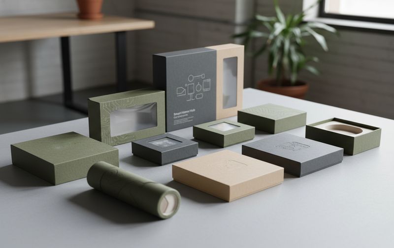
Custom Packaging for Electronic Components and Gadgets
In the highly competitive and rapidly evolving United Kingdom market, the role of custom packaging for electronic components and gadgets extends far beyond mere containment. It is a critical strategic element that safeguards product integrity, reinforces brand identity, and optimises supply chain efficiency. Businesses operating within the UK, from burgeoning startups to established multinational corporations, understand that generic, off-the-shelf packaging solutions simply do not suffice for the intricate and often fragile nature of modern electronics. Instead, a tailored approach to packaging ensures that sensitive components arrive at their destination free from damage, compliant with rigorous industry standards, and ready for integration or retail. This proactive investment in bespoke packaging not only mitigates potential financial losses associated with damaged goods and returns but also enhances a company’s reputation for quality and reliability, fostering stronger relationships with B2B partners and end-consumers alike.
Navigating the complexities of electronics packaging requires a deep understanding of material science, logistics, and regulatory requirements specific to the UK. Every aspect, from the choice of anti-static materials to the precision of labeling, plays a pivotal role in the overall success of a product’s journey from manufacturing to its final user. Ultimately, effective custom packaging for electronic components and gadgets becomes an invaluable asset, allowing businesses to differentiate themselves, ensure operational continuity, and maintain a competitive edge in a demanding market. By prioritising intelligent packaging design, companies can confidently deliver their cutting-edge technology, secure in the knowledge that their products are protected every step of the way, upholding both their value proposition and their commitment to excellence.
Electronic Component Packaging
Investing in tailored electronic component packaging is not merely a cost; it is a crucial strategic decision for safeguarding product integrity, enhancing brand perception, and optimising operational efficiency within the United Kingdom market. The inherent sensitivity and often diminutive size of electronic components mean that generic, one-size-fits-all packaging solutions are inherently prone to failure. Such failures can manifest as physical damage from impacts, vibrations, or compression during transit, leading to costly returns, rework, and ultimately, a tarnished brand reputation. Imagine a shipment of high-value integrated circuits arriving with bent pins or micro-fractures; the financial repercussions and delays for the receiving manufacturer can be substantial. Custom packaging, by contrast, is meticulously engineered to cradle each component precisely, accounting for its unique vulnerabilities and ensuring it remains pristine from the moment it leaves the production line until it is integrated into a final product or gadget.
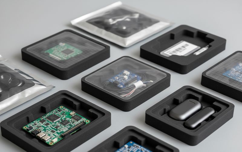
The reasoning behind this tailored approach lies in the diverse nature of electronic components themselves. A delicate PCB requires different protection than a robust power supply unit. Off-the-shelf options, designed for broad applicability, often result in either over-packaging—leading to unnecessary material waste and increased shipping costs—or, more dangerously, under-packaging, leaving components vulnerable. A truly custom solution begins with a thorough assessment of the product’s specific vulnerabilities, encompassing factors such as electrostatic discharge (ESD) sensitivity, susceptibility to shock and vibration, and intolerance to moisture. This granular understanding then informs the selection of appropriate materials and design techniques. For instance, precisely cut foam inserts (made from materials like polyethylene or polyurethane) can absorb shocks, while custom-moulded pulp trays offer a sustainable, form-fitting solution for a multitude of components. For items requiring a higher level of rigidity and protection against crushing, corrugated cardboard boxes with custom partitions are often employed. The goal is always to create a protective environment that precisely matches the component’s needs, preventing movement within the package and mitigating external stresses.
To implement effective custom electronic component packaging, businesses in the UK should follow several actionable steps. Firstly, conduct a detailed vulnerability assessment for each component type, ideally with input from engineering and logistics teams. Secondly, explore a range of material science options, balancing protection with sustainability goals; many modern packaging solutions offer recycled content or are fully recyclable, appealing to the environmentally conscious UK market. Thirdly, consider the unboxing experience, even for B2B clients, as well-presented components reflect positively on the supplier’s professionalism and attention to detail. This might involve clear labeling and easy-to-access compartments. Finally, partner with a reputable packaging manufacturer that possesses expertise in electronics and understands UK market nuances and regulatory standards. Potential pitfalls include ignoring the importance of sustainability (which is increasingly scrutinised in the UK), designing packaging that is too complex for efficient assembly lines, or failing to test the packaging under simulated transport conditions. Solutions to these challenges involve an iterative design process, seeking expert advice early on, and prioritising ease of use and environmental impact alongside robust protection.
| Material Type | Key Protective Qualities | Typical Applications | Cost Efficiency | Sustainability Notes |
|---|---|---|---|---|
| Corrugated Cardboard | Structural integrity, cushioning (with inserts), stackability. | Outer boxes, internal dividers, component trays. | High (very cost-effective). | High (often recycled/recyclable). |
| Polyethylene (PE) Foam | Excellent shock absorption, vibration dampening, moisture resistance. | Custom-fit inserts for delicate PCBs, hard drives, sensors. | Medium to High. | Some recyclable options, often made from virgin material. |
| Polypropylene (PP) Containers | Rigid protection, chemical resistance, reusability, ESD options. | Component bins, reusable trays, shipping containers. | Medium to High (for durability). | Reusable, some recyclable options. |
| Moulded Pulp | Conformable cushioning, sustainable, lightweight. | Custom inserts for small gadgets, specific components. | Medium. | Very High (recycled paper, compostable). |
This table illustrates the diverse array of materials available for custom packaging solutions specifically designed for electronic components. Each material offers a unique set of properties, allowing businesses to select the optimal combination for their specific product and supply chain requirements in the UK. Understanding these characteristics helps in making informed decisions that balance protection, cost, and environmental responsibility, ensuring the chosen custom packaging aligns perfectly with the component’s needs.
Anti Static

For businesses handling electronic components and gadgets in the UK, implementing robust anti-static packaging is not merely an option; it is an absolute imperative. Electrostatic discharge (ESD) remains one of the most insidious and costly threats to modern electronics, capable of inflicting severe, often invisible, damage that can cripple components before they even reach their intended application. The takeaway here is clear: essential for sensitive electronic components, anti-static packaging prevents costly ESD damage, ensuring product functionality and reliability upon arrival. Without proper ESD protection, components might suffer latent defects that manifest as intermittent failures down the line, leading to expensive warranty claims, product recalls, and significant reputational damage. The ever-decreasing size and increasing sensitivity of semiconductor devices mean that even a small static spark, imperceptible to humans, can render a component useless, making comprehensive anti-static measures critical across the entire supply chain.
The reasoning behind this urgency stems from the nature of ESD itself. Static electricity is generated through friction (tribocharging) and can accumulate on surfaces, personnel, or even non-conductive packaging materials. When a charged object comes into contact with a sensitive electronic component, a rapid transfer of charge occurs, generating a surge of current that can permanently alter or destroy the delicate internal circuitry. The hidden costs of ESD damage are particularly pernicious. Beyond the obvious expense of replacing damaged components, there are costs associated with troubleshooting, production line stoppages, failed final product tests, and the intangible yet significant loss of customer trust. Modern electronic components can be damaged by discharges as low as 10-100 volts, while the human body can generate thousands of volts without feeling a shock. This disparity underscores the necessity for specialised anti-static packaging materials that either dissipate static charges safely, shield components from external fields, or prevent charge generation in the first place.
To effectively mitigate ESD risks, businesses engaged in custom packaging for electronic components and gadgets in the UK should adopt several actionable steps. Firstly, identify all components that are ESD-sensitive and categorise them by their susceptibility levels. Secondly, understand the different types of anti-static material available: conductive materials (which quickly drain charges), static-dissipative materials (which slowly dissipate charges), and static-shielding materials (which create a Faraday cage effect). Each has a specific role, often used in combination. For instance, anti-static bags, typically made from dissipative or shielding plastics, are widely used for individual components, while conductive foam inserts can safely hold multiple pins. Thirdly, specify anti-static custom packaging solutions from suppliers who adhere to international standards like IEC 61340-5-1, ensuring consistent and reliable protection. Fourthly, consider the entire anti-static supply chain, including handling procedures, grounding protocols, and even anti-static flooring in storage areas. Potential pitfalls include relying on “pink anti-static” materials that may lose their properties over time or providing insufficient shielding for highly sensitive devices. Another common mistake is not regularly testing anti-static packaging to ensure it still meets specifications. Solutions involve continuous training for staff, regular audits of packaging materials, and partnering with specialist suppliers who can provide certified ESD-safe custom packaging for electronic components and gadgets.
B2B Supply
Optimised custom packaging is a cornerstone for streamlining B2B supply chains in the UK, moving beyond mere protection to encompass crucial aspects of logistics, efficiency, and the cultivation of robust supplier relationships. For businesses dealing with electronic components and gadgets, generic packaging can become a significant bottleneck, increasing handling times, storage complexities, and freight costs. The takeaway is clear: tailored custom packaging streamlines B2B supply chains, reducing logistics costs, improving handling, and fostering strong supplier relationships. In a market where just-in-time delivery and lean manufacturing principles are paramount, packaging that facilitates quick identification, easy handling, and efficient storage translates directly into a competitive advantage. Imagine a warehouse struggling to identify component batches due to inconsistent labeling, or a production line slowed by components that are difficult to extract from their packaging; these inefficiencies erode profitability and damage a supplier’s reputation.
The reasoning behind customisation for B2B supply centres on integration and collaboration. Unlike retail packaging, which often prioritises consumer appeal, B2B custom electronic packaging must integrate seamlessly into the client’s operational workflow. This means considering how components will be received, stored, and ultimately used. For example, trays designed for automated pick-and-place machines reduce manual handling and errors. Bulk packaging solutions, such as returnable plastic containers or large corrugated boxes with custom inserts, can significantly reduce waste and consolidate shipments, lowering transportation costs and environmental impact. Furthermore, packaging designed for optimal palletisation ensures maximum load efficiency, minimising empty space in lorries and warehouses. This proactive approach to packaging design, often developed in close consultation with B2B clients, demonstrates a commitment to their operational success, strengthening partnerships and fostering long-term contracts. It’s about creating an entire system that supports the flow of goods, not just individual product protection.
To effectively leverage custom packaging for electronic components and gadgets in B2B supply, businesses should implement several actionable steps. Firstly, design packaging for optimal warehousing and transport efficiency, focusing on standard dimensions, stackability, and unit load integrity. This includes using packaging materials robust enough to withstand multiple handling points and stacking pressures. Secondly, incorporate features that facilitate easy handling and identification at every stage, such as ergonomic hand holes, clear instructional markings, and large, scannable barcodes. Thirdly, explore solutions for reusability or recyclability, especially for returnable packaging systems, aligning with UK sustainability targets and offering cost savings over time. Collaboration with logistics partners and end-users on packaging design is crucial to gather insights into their specific operational needs and challenges. Potential pitfalls include designing non-standard dimensions that lead to wasted space or increased freight costs, ignoring the specific environmental conditions components might face in transit or storage, or creating packaging that is overly complex and time-consuming to open at the receiving end. Solutions involve adopting modular packaging systems, conducting thorough transit testing to ensure durability, and prioritising simplicity and functionality alongside protection. By focusing on these elements, businesses can transform their custom packaging from a protective necessity into a powerful tool for supply chain optimisation.
| Consideration | Benefit of Customisation | Potential Pitfall (without customisation) |
|---|---|---|
| Stackability & Dimensions | Optimises warehouse space and freight volume, reduces crushing risk. | Wasted space, unstable stacks, increased shipping costs. |
| Ease of Handling | Reduces labour time, minimises risk of damage during manual handling. | Slow processing, ergonomic issues, increased product damage. |
| Material & Durability | Ensures multi-trip use (for reusables), protects against transit stresses. | Frequent damage, high replacement costs, short lifecycle for packaging. |
| Information & Labeling | Clear identification, compliance, efficient inventory management. | Misidentification, processing delays, regulatory fines. |
| Sustainability | Meets UK environmental goals, appeals to eco-conscious partners. | Increased waste, negative brand perception, higher disposal costs. |
This table highlights the critical factors that UK businesses must address when designing custom packaging for electronic components and gadgets for B2B supply. Each customisation offers tangible benefits that directly impact operational efficiency and cost-effectiveness. Neglecting these considerations can lead to significant inefficiencies and financial drawbacks, reinforcing the strategic importance of a bespoke packaging approach in the business-to-business sector.
Labeling
Accurate and comprehensive labeling on custom packaging for electronic components and gadgets is far more than a simple formality; it is an indispensable element for efficient inventory management, ensuring strict regulatory compliance, and providing vital information to the end-user throughout the UK supply chain. The clear takeaway here is that precise labeling is critical for inventory management, regulatory compliance, and consumer information. Inadequate or erroneous labeling can trigger a cascade of negative consequences, from shipment delays and misrouted products to hefty regulatory fines and significant customer dissatisfaction. Imagine a batch of mission-critical components held up at customs due to missing UKCA marking, or a technician wasting hours trying to identify a part because the batch number is illegible. Such scenarios underscore the profound impact that meticulous labeling has on operational fluidity and market credibility within the highly regulated UK landscape.
The reasoning behind the paramount importance of detailed labeling stems from the complex journey electronic products undertake. From the manufacturing floor to warehouses, distribution centres, and finally to the assembly line or end-consumer, each stage relies heavily on the information conveyed by the label. For B2B shipments of electronic components, labels must often include product identification numbers, serial numbers, batch codes, manufacturer details, country of origin, and critical safety warnings or handling instructions. For consumer gadgets, labeling extends to regulatory marks like CE and UKCA, WEEE (Waste Electrical and Electronic Equipment) symbols, battery disposal instructions, and energy efficiency ratings. Furthermore, in an increasingly globalised supply chain, multi-language labels may be required. The durability of these labels is equally critical; they must withstand varying environmental conditions, abrasion, and moisture without fading or detaching, preserving readability throughout the product’s lifecycle. This attention to detail ensures that components can be precisely tracked, correctly identified, and handled according to their specific requirements, preventing costly errors and ensuring compliance with stringent UK and international standards.
To ensure effective labeling for custom packaging of electronic components and gadgets, businesses in the UK should adopt a methodical approach. Firstly, identify all necessary information for each product type, which typically includes product ID, serial and batch numbers, manufacturer information, safety warnings (e.g., “ESD Sensitive”), and all relevant certifications (CE, UKCA, RoHS, WEEE). Secondly, select appropriate label materials and adhesives that are durable and suited to the specific environment the packaging will encounter, considering factors like temperature, humidity, and abrasion. Thirdly, integrate scannable barcodes or QR codes to facilitate seamless inventory tracking and supply chain management, crucial for automated systems. Fourthly, ensure strict compliance with all UK regulations, including the proper display of UKCA marking for products placed on the Great Britain market, and WEEE directive symbols for end-of-life disposal. It is vital to regularly review and update labeling requirements, as regulations can change. Potential pitfalls include using generic, non-compliant labels, placing labels in difficult-to-scan locations, or using materials that are prone to fading or peeling, leading to illegible information. Solutions involve implementing automated labeling systems for consistency and speed, utilising digital printing for variable data, and collaborating with packaging experts who are knowledgeable about the latest UK regulatory frameworks and best practices for creating resilient, compliant, and informative labels for electronic products.
Protection
Robust protection through custom packaging is an absolute, non-negotiable requirement for electronic components and gadgets, safeguarding them from a multitude of physical and environmental threats throughout their entire journey within the UK and beyond. The unwavering takeaway is that comprehensive protection, delivered via custom packaging, shields products from physical damage, environmental factors, and tampering, securing their integrity. Generic packaging solutions frequently fall short in addressing the diverse vulnerabilities of electronics, leaving them susceptible to impacts, vibrations, compression, moisture, dust, and electrostatic discharge. Any compromise in protection can lead to catastrophic consequences: damaged goods, increased return rates, warranty claims, lost revenue, and, critically, a damaged brand reputation in a market that demands reliability and quality. Investing in packaging engineered for specific protective challenges is not an overhead; it is a fundamental pillar of product quality assurance and business continuity.
The reasoning for this stringent focus on protection stems from the inherent fragility and value of electronic components and gadgets. Modern electronics, with their intricate circuitry and delicate interconnections, are highly vulnerable to physical shocks. A drop or harsh impact can cause internal fractures, component dislodgements, or bent pins. Constant vibration during transit can lead to fatigue in solder joints or micro-fractures in circuit boards. Compression from stacking in warehouses or during shipment can crush sensitive displays or distort casings. Beyond physical forces, environmental factors pose significant threats; moisture can lead to corrosion or short circuits, while dust can impede functionality or cause overheating. Moreover, for high-value gadgets, protection against tampering is also paramount, ensuring product authenticity and security. A holistic custom packaging design addresses all these threats systematically, employing a multi-layered approach where each packaging element serves a specific protective function, working in concert to create an impenetrable shield around the product. This comprehensive strategy minimises the risk of damage, reduces waste, and ultimately lowers the total cost of ownership by preventing costly post-delivery issues.
To implement truly effective protection for electronic components and gadgets via custom packaging, businesses in the UK must take several actionable steps. Firstly, conduct rigorous drop, vibration, and compression testing using industry standards (e.g., ISTA protocols) to simulate real-world shipping and handling conditions. This data is crucial for validating packaging designs. Secondly, select appropriate cushioning materials based on the product’s fragility and weight; options range from precisely engineered foam inserts (like polyethylene or polyurethane) that absorb high levels of shock, to air pillows that fill voids and prevent movement, or corrugated inserts that provide structural support. Thirdly, incorporate moisture barriers, such as desiccant packs within sealed barrier bags or films, to protect humidity-sensitive components. Fourthly, for high-value gadgets or items containing sensitive data, integrate tamper-evident features like seals or security tapes to deter and detect unauthorised access. Finally, design the outer packaging for optimal stacking strength, ensuring it can withstand the compressive forces of palletisation without deforming or damaging the contents. Potential pitfalls include underestimating the severity of transit hazards, using generic cushioning materials that don’t match the product’s fragility, or neglecting environmental factors like extreme temperature fluctuations. Solutions involve partnering with packaging engineers who specialise in electronics, continuously monitoring packaging performance, and embracing innovative materials like smart packaging that can indicate if damage has occurred in transit, providing invaluable data for continuous improvement in custom packaging for electronic components and gadgets.
| Protection Challenge | Risk to Electronic Components/Gadgets | Custom Packaging Solution Example |
|---|---|---|
| Impact / Shock | Cracked PCBs, dislodged components, broken screens, internal damage. | Precision-cut PE/PU foam inserts, suspension packaging, moulded pulp trays. |
| Vibration | Fatigue in solder joints, component lead damage, fretting corrosion. | Resilient foam cushioning, custom corrugated inserts that isolate movement. |
| Compression / Crushing | Deformed casings, crushed components, damaged displays, short circuits. | High-strength corrugated boxes (e.g., triple-wall), internal support structures. |
| Moisture / Humidity | Corrosion, short circuits, mold growth, reduced component lifespan. | Sealed barrier bags (e.g., metallised foil), desiccant packs, anti-corrosion VCI papers. |
| Electrostatic Discharge (ESD) | Latent or catastrophic component failure, invisible damage. | Anti-static bags, conductive/dissipative foam, ESD-safe containers/trays. |
| Dust / Contamination | Impaired functionality, overheating, reduced lifespan, cosmetic damage. | Sealed bags, clear plastic clamshells, dust-resistant inner wraps. |
This table provides a concise overview of the primary protection challenges faced by electronic components and gadgets and how custom packaging solutions effectively mitigate each risk. By tailoring packaging to address these specific vulnerabilities, businesses ensure their products are shielded from the moment they leave the factory until they reach their final destination, a critical factor for success in the demanding UK market. This targeted approach is far more effective than generic packaging, which often leaves products exposed to one or more of these detrimental factors.